
Silicon dominates the photo voltaic electricity landscape, but it isn’t the best materials for creating skinny, light-weight photo voltaic cells needed for satellites and drones.
Atomically skinny semiconducting resources this sort of as tungsten diselenide and molybdenum disulfide, which are previously getting deemed for subsequent-technology electronics, hold promise for lower-price ultrathin photo voltaic cells that can also be flexible. And now, engineers have built tungsten diselenide photo voltaic cells that boast a electricity-for every-weight ratio on par with recognized skinny-movie photo voltaic cell technologies.
The flexible photo voltaic cells claimed in the journal Character Communications have a light-weight-to-electricity conversion effectiveness of five.1 per cent, the best claimed for flexible cells of this variety. Their unique electricity, meanwhile, is four.four W/g, equivalent with skinny-movie photo voltaic cells—such as all those built of cadmium telluride, copper indium gallium selenide, amorphous silicon, and III-V semiconductors. With additional engineering to lessen the substrate thickness and growing effectiveness, the technology has the opportunity to get to 46 W/g, “way outside of what has been demonstrated for other photovoltaic technologies,” suggests Koosha Nassiri Nazif, an electrical engineer at Stanford University who led the function with his colleague Alwin Daus.
It is a thousand moments thinner than silicon but with the exact amount of money of absorption as a typical silicon wafer.
Silicon’s effectiveness is tricky to beat for the price, and silicon photo voltaic panel costs have been dropping every single calendar year. But “silicon is rather suboptimal for emerging programs,” Nassiri Nazif suggests. These kinds of programs include wearable and conformable electronics, wise windows and other architectural works by using, unmanned aerial motor vehicles, and electrical motor vehicles. “Another significant application is the World wide web of Issues,” he suggests, “where you can prolong the battery everyday living or absolutely clear away need for batteries to electricity tiny sensors and products.”
Substantial unique electricity is crucial for all those works by using, he suggests. Today’s skinny-movie technologies and newer perovskite photo voltaic cells all have greater unique electricity than silicon, with perovskites keeping the history at 29 W/g.
But tungsten diselenide and molybdenum disulfide, which belong to a class of resources known as transition metallic dichalcogenides (TMD), have rewards above other resources. They are additional light-weight than the skinny-movie CdTe or CIGS cells applied in aerospace now. They’re also additional steady than perovskites and organic photovoltaic materials—and are additional environmentally pleasant than lead-containing perovskites.
Moreover, TMD resources boast some of the best light-weight absorption abilities of any photovoltaic materials. “So you can have an ultrathin layer a thousand moments thinner than silicon and however have the exact amount of money of absorption with correct optical layout,” Nassiri Nazif suggests.
Nevertheless, the best TMD photo voltaic cells so significantly have had efficiencies a lot less than 3%, and a lot less then .7% when built on a light-weight, flexible substrate. The materials’ theoretical effectiveness, nevertheless, is 27%. Daus suggests they are simply just newer on the scene and need additional heavy engineering to strengthen effectiveness. All photovoltaic resources experience charge-extraction challenges. That is, once the materials absorbs a photon and creates electrons and holes, all those charge carriers have to be speedily extracted ahead of they can recombine.
The trick is to find the right get in touch with materials to shuttle the charge carriers from the semiconductor to the electrodes. The scientists selected a transparent graphene sheet for that. Then they coated it with a molybdenum oxide layer, which is also transparent and boosts graphene’s skill to extract charge carriers, Daus explains.
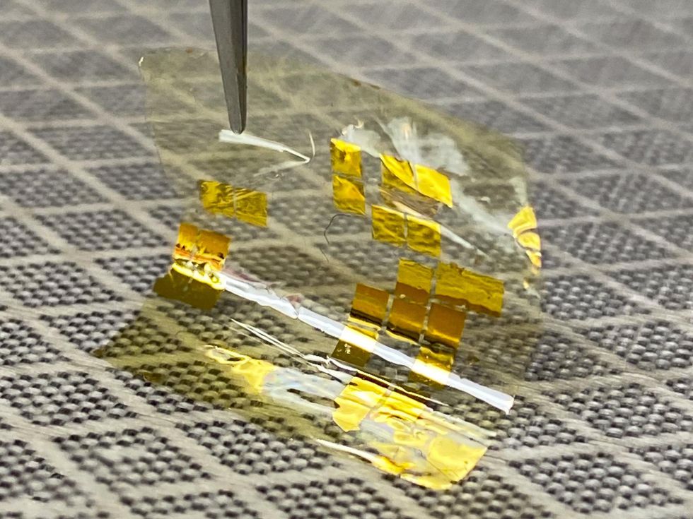
An additional essential advance that allows them make higher-top quality flexible photo voltaic cells is the transfer method they have formulated, he adds. They initial deposit tungsten diselenide flakes on a silicon substrate, deposit gold electrodes on it, and then coat it with a skinny flexible plastic substrate. Then they put the entire ensemble in a water bathtub to carefully peel off the flexible construction from the silicon. Ultimately, they flip the construction above so the tungsten diselenide is on major, and coat it with the graphene and molybdenum oxide. The entire system in the finish is only 350 nm thick.
The photo voltaic cells are small at this position, Nassiri Nazif factors out, about a hundred x a hundred µm. “To get to the position where by it can be commercialized, we need at least 1 x 1 cm products,” he suggests. “The very good news is that large-location, higher-top quality TMD development has previously been demonstrated.”
But most efforts have centered on creating monolayer TMD resources for electronics, suggests Daus, whereas for photo voltaic cells you need thicker 100–200 nm movies. The Stanford group has previously beginning creating two x two cm movies of TMDs, but so significantly the thicker movies have not achieved the exact higher top quality as the smaller sized flakes they applied in the paper
They hope that this function evokes additional exploration in the location of TMD photo voltaic cells. “Our intention is to create a foundation for TMD photovoltaic programs,” Nassiri Nazif suggests. “These resources have a fundamental gain above other technologies. If we clear up the engineering challenges, it could be the materials of selection for subsequent-technology photovoltaic technology.”